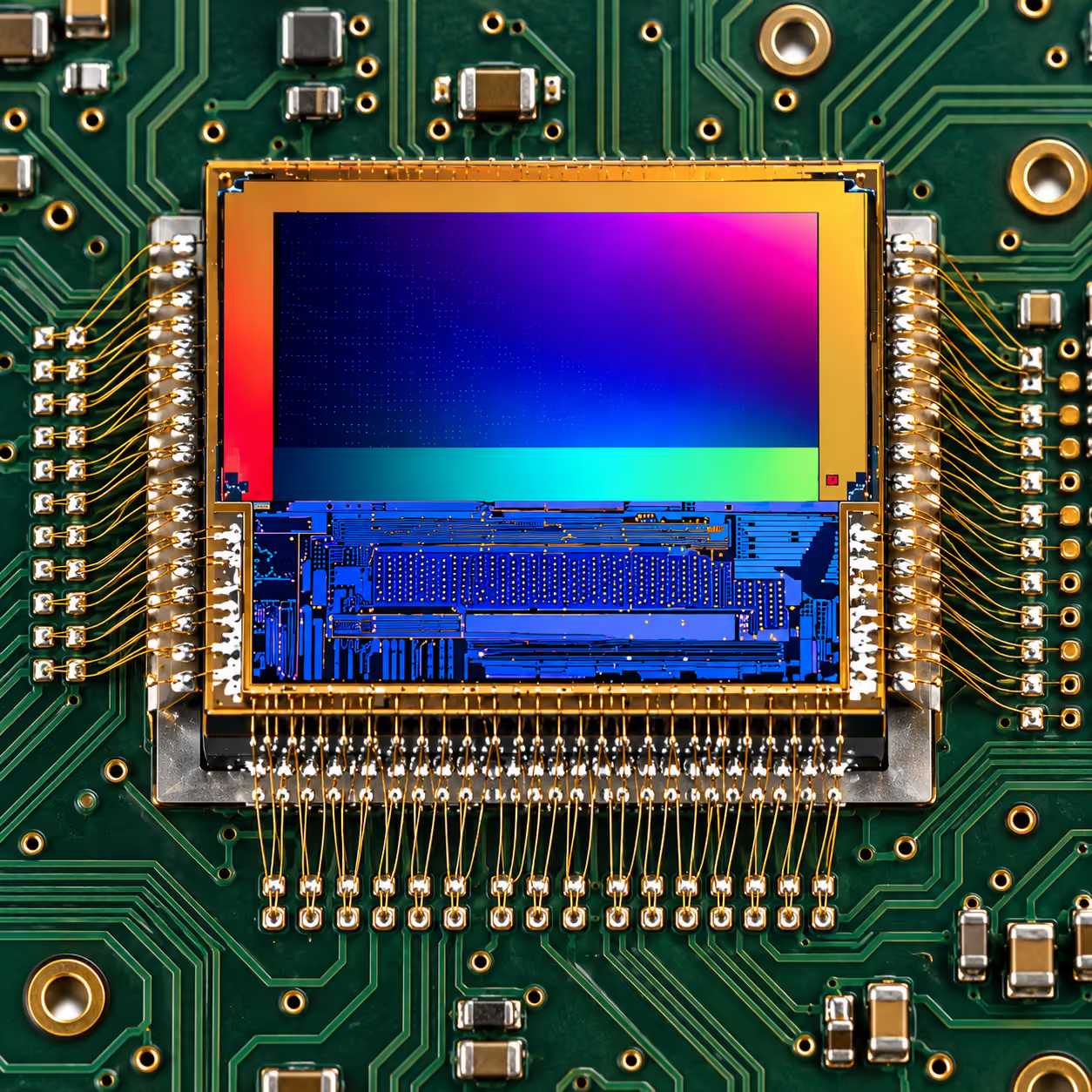
U.S.-based wafer processing, semiconductor assembly, and packaging—from precision wafer dicing and die placement to wire bonding, flip-chip assembly, substrates, and testing.
NFR combines in-house manufacturing with direct engineering support for prototypes, low-volume builds, and specialized semiconductor programs. Engage us for a single process or a coordinated path from fabricated wafer to assembled and tested device.

Support for:
Domestic capabilities and in-house processes reduce traditional OSAT lead times.
Work directly with engineers who understand design, packaging, substrates, RF, and test.
U.S.-based, ITAR-capable services for programs where supply-chain control matters.
The specifications below represent common NFR capabilities and are intended as a starting point. Our engineering team regularly supports requirements, materials, package formats, and processes outside these ranges.
250 µm × 250 µm
50 µm–1 mm
60 µm
±5 µm
Conductive and non-conductive
10 µm
Flip-chip, multi-die/module placement, C4 reflow, Au thermal compression bonding, underfill
QFN, leadframe, open cavity, chip-on-board and other package formats
Application and selective removal
Available
40 µm
Ball, wedge and ribbon
Typically 1–3 business days for standard orders
ISOLA 370HR, KINGBOARD KB-6167F, ISOLA ASTRA MT77
Up to 12.5 mm × 12.5 mm
1–8 layers
2 mil / 2 mil ≈ 50 µm / 50 µm
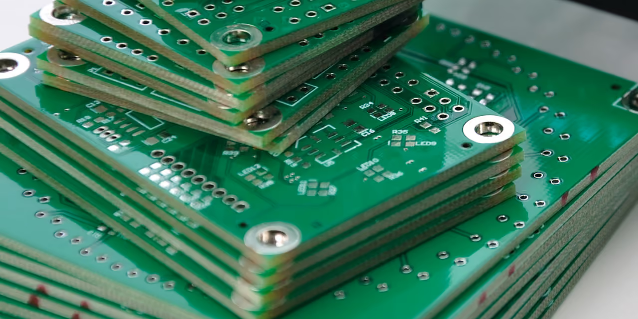
NFR's in-house substrate manufacturing eliminates one of the most common bottlenecks in advanced packaging. Rapid-turn substrates and interposers can be produced in as little as 1–3 business days, helping packaging, integration, and testing move forward faster.
Many specialized packaging programs require processes that go beyond assembly alone. NFR's in-house cleanroom capabilities support wafer, die, substrate, and packaging workflows with processes including photolithography, deposition and metallization, etching, inspection, and metrology.
Whether used as part of an integrated OSAT program or as a standalone service, these capabilities give NFR greater flexibility to develop, modify, and support processes for specialized semiconductor programs.

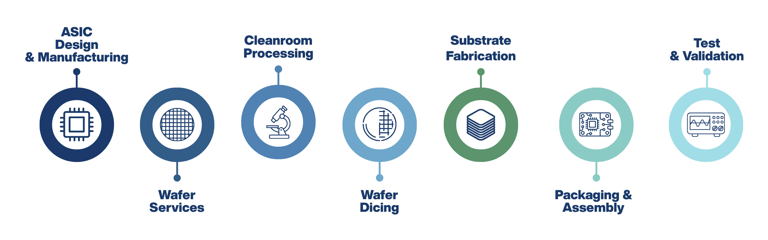
NFR can support a semiconductor program before and after packaging. ASIC and package design, wafer processing, cleanroom services, dicing, substrate fabrication, packaging, bring-up, and testing can be accessed individually or coordinated as one development path.
ENGINEERING-LED SOLUTIONS
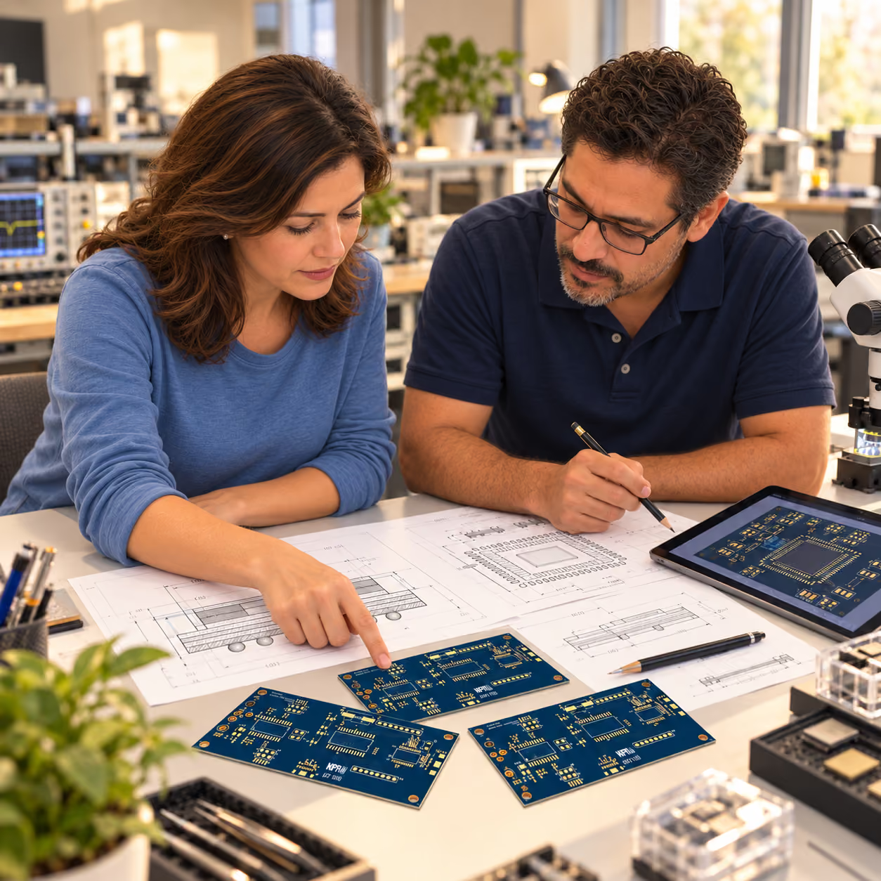
NFR's engineers work directly with customers on specialized packaging, integration, substrate, RF, and test challenges that may not fit a traditional OSAT process flow. We can help evaluate the problem, develop the process, build prototypes, characterize the results, and refine the solution.
Whether you need a single specialized process, rapid prototype packaging, or an integrated path from ASIC design through test, NFR can help determine the fastest and most practical approach.


Yes. NFR's U.S.-based OSAT capabilities provide packaging, assembly, and testing, including wire bond, flip-chip, and 2.5D integration.
Large OSATs are generally optimized for high-volume semiconductor production. NFR's OSAT is designed for smaller, specialized programs that need greater flexibility, engineering collaboration, rapid turnaround, and lower-volume support.
NFR's wafer processing and semiconductor packaging services are particularly suited to organizations developing prototypes, custom ASICs, specialized semiconductor devices, research programs, and low-volume or emerging production programs that may not fit the business model of a large global OSAT.
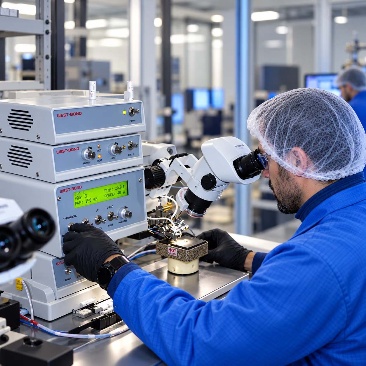
NFR's capabilities include flip-chip assembly, wire bonding, die attach, C4 reflow, gold thermal compression bonding, underfill, BGA solder bump application, multi-module placement, gold stud bumping, and conventional packaging approaches such as QFN and lead-frame packaging.
Yes. NFR supports lead-frame, open-cavity, and chip-on-board wire bonding, conductive and non-conductive die attach, and ball, wedge, and ribbon bonding.
Yes. Flip-chip and C4 assembly are part of NFR's advanced packaging capabilities, along with underfill, bumping, and related integration processes.
Yes. NFR manufactures specialized substrates and interposers in-house. This can significantly reduce the substrate lead times that often delay prototype packaging programs.
Yes. NFR provides precision dicing for silicon, glass, and advanced substrates, including fast-turn prototyping and specialized processing for fragile materials.
Yes. We can support the path from fabricated wafer through dicing, packaging, substrate development, assembly, testing, PCB integration, bring-up, and production planning.
Yes. Supporting prototypes and smaller-volume programs is a core reason for NFR's OSAT model. Customers can access advanced packaging capabilities without requiring the production volumes typically associated with a large OSAT.
Yes. Because NFR's engineering capabilities span ASIC design, packaging, substrates, PCB integration, and testing, we can consider electrical, mechanical, thermal, manufacturing, and system requirements when developing a packaging approach.
Yes. NFR can support wafer processing and dicing, package and substrate development, assembly, PCB development, bring-up, validation, testing, and production support, providing continuity beyond tape-out.
Yes. NFR's wafer processing and semiconductor packaging services are U.S.-based and designed to provide responsive engineering collaboration, faster turnaround, and domestic supply-chain options for programs where those considerations matter.