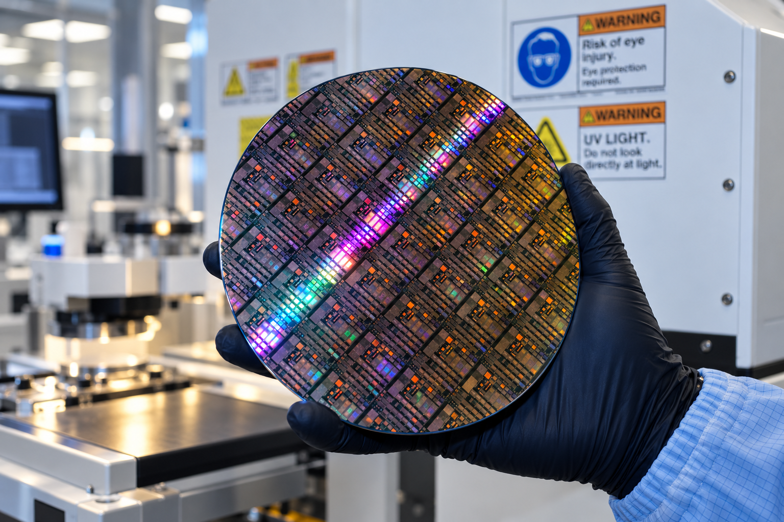
U.S.-based cleanroom processing for semiconductor development, wafer preparation, microfabrication, prototyping, and specialized production.
NFR provides cleanroom and wafer processing capabilities for semiconductor programs that require precision, flexibility, and direct engineering support.
Engage NFR for a specific process or integrate cleanroom services into a broader development program spanning wafer processing, advanced packaging, assembly, and test.
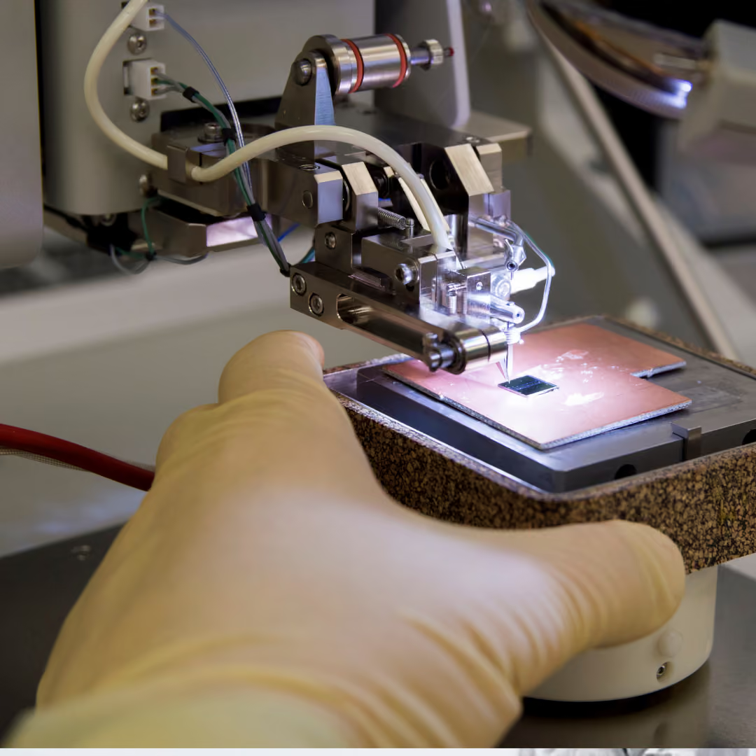
Precision dicing for silicon, glass, and advanced substrates, supporting individual process requirements from engineering samples through production quantities.
Specialized handling and processing for wafers, bare die, and advanced substrates within NFR's controlled cleanroom environment.
Capabilities support semiconductor development programs where standard high-volume manufacturing processes may not provide the flexibility required.
NFR supports specialized microfabrication and wafer-level processes for development, prototyping, and low-volume semiconductor programs.
Cleanroom capabilities extend into precision die and component placement for programs requiring integration with substrates, packages, or multi-component assemblies.
Available processes include multi-module placement with accuracy to 10 µm.
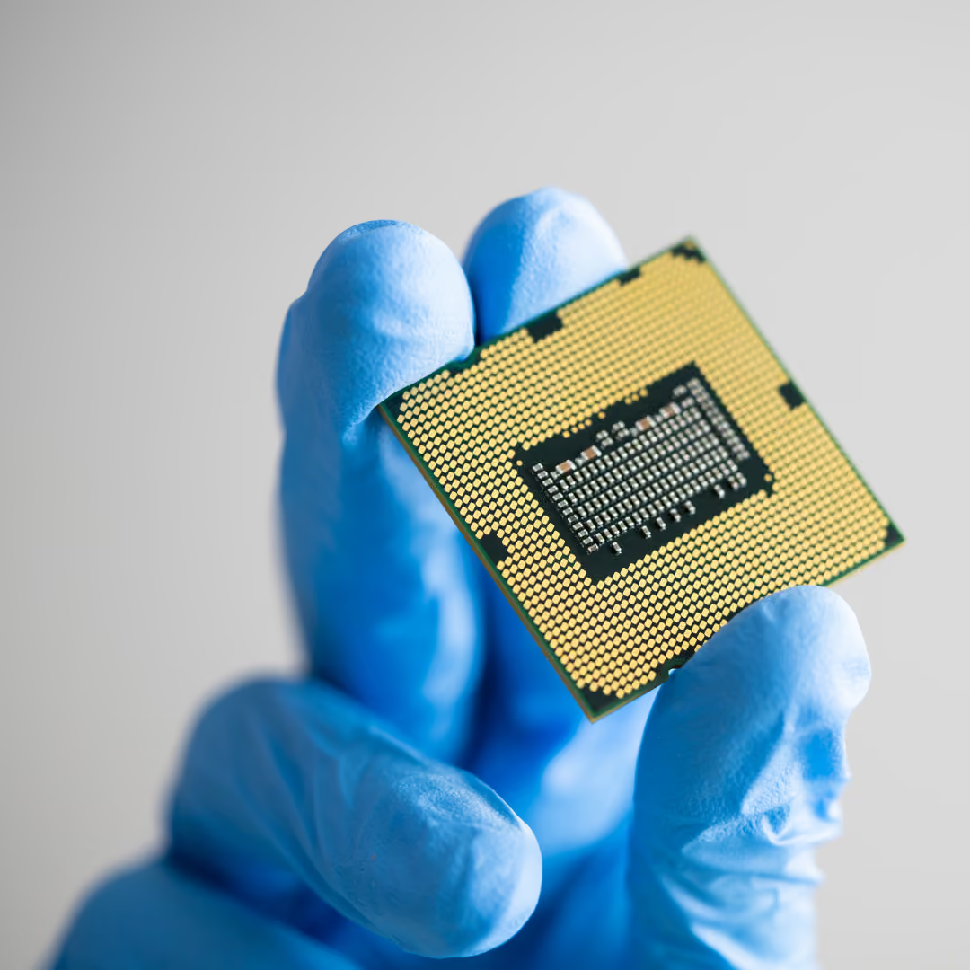
IN-HOUSE SUBSTRATE FABRICATION
When a project moves beyond wafer or die processing, NFR can continue the development path through standard and advanced packaging, assembly, substrates, and test with its U.S.-based micro-OSAT.
ENGINEERING-LED SOLUTIONS
NFR's cleanroom isn't an isolated capability. It operates within a broader semiconductor development organization.
That gives customers access to engineering expertise across ASIC design, substrates, PCB development, wafer processing, advanced packaging, assembly, and test.
For programs that span multiple disciplines, keeping those capabilities connected can reduce handoffs, identify integration challenges earlier, and accelerate the transition from development to production.
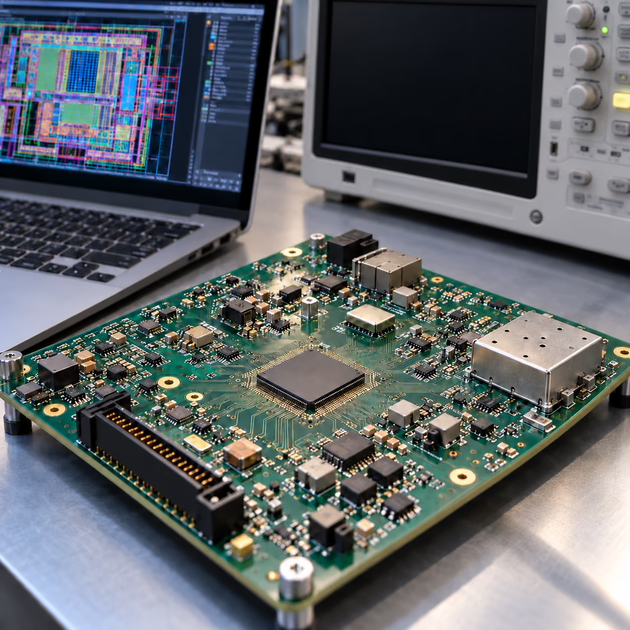

From a single cleanroom process to an integrated semiconductor development program, NFR can build an engagement around your technical requirements.