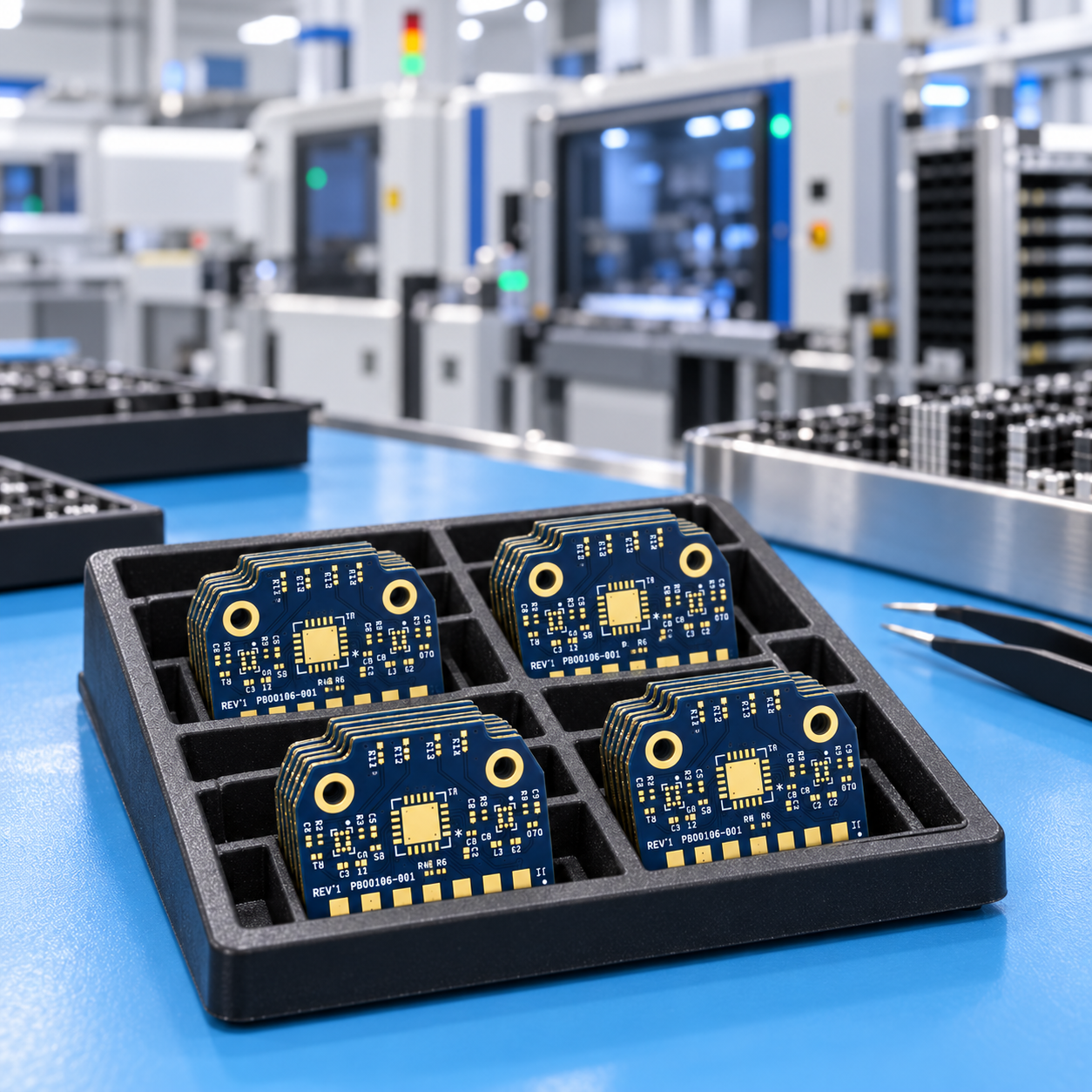
From rapid prototypes to production-ready boards, NFR delivers reliable PCBs and substrate manufacturing with responsive engineering support.













2-layer boards in 2 business days.
4-layer boards in 3 business days.
Fast-turn options available for more complex designs.
Domestic, ITAR-registered and ISO 9001-certified manufacturing with responsive communication.
Hybrid stack-ups, controlled impedance, and specialized materials for demanding RF, microwave, and high-speed applications.
Direct access to engineers who can review designs and identify manufacturability issues before production.
Bondable ENIG and application-specific finishes supporting conventional assembly and advanced packaging.
FR-4, high-frequency RF laminates, ceramic substrates, and specialty materials.
Whether you arrive with a completed design or need engineering support, NFR can take your PCB from initial requirements through fabrication and production.
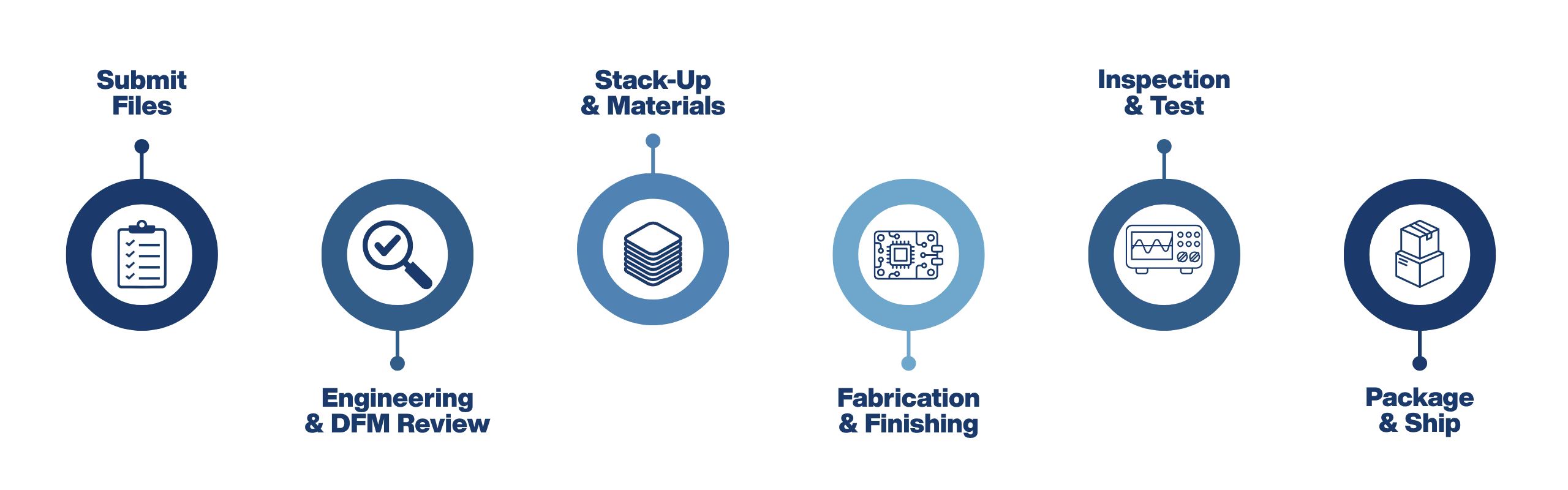
Don't see your requirements below? These are our standard online-order specifications.
Contact our PCB team for custom materials, dimensions, layer counts, finishes, and advanced requirements.
Controlled-impedance stack-ups, RF laminates, hybrid material constructions, and engineering support for demanding RF and microwave applications.
Stack-ups and material selection engineered around signal integrity and demanding digital performance.
Rapid-turn substrates supporting wire bond, flip-chip, BGA, and other semiconductor packaging requirements.
Specialized materials, finishes, geometries, and configurations for requirements outside standard PCB fabrication.
Have an unusual board requirement?
Need Something Outside Our Standard Specifications?
NFR can support a wide range of PCB materials, configurations, and requirements.
Orders outside our standard specifications may require additional lead time.
Talk with our PCB team to discuss your requirements and available turnaround options.

Start with one of our standard configurations for the fastest turnaround, or work with NFR to develop a custom stack-up for your electrical, RF, thermal, or mechanical requirements.

Need something outside our standard specifications?
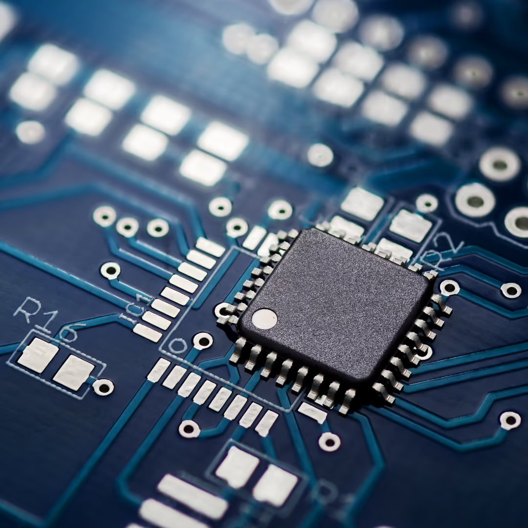
NFR's PCB and substrate capabilities are part of a broader semiconductor development ecosystem. For programs requiring standard or advanced packaging, NFR can continue with substrate fabrication, die attach, wire bonding, flip-chip integration, assembly, and test through our U.S.-based OSAT capabilities.
NFR engineers can support schematic development, layout, stack-up, DFM, and design optimization before fabrication.
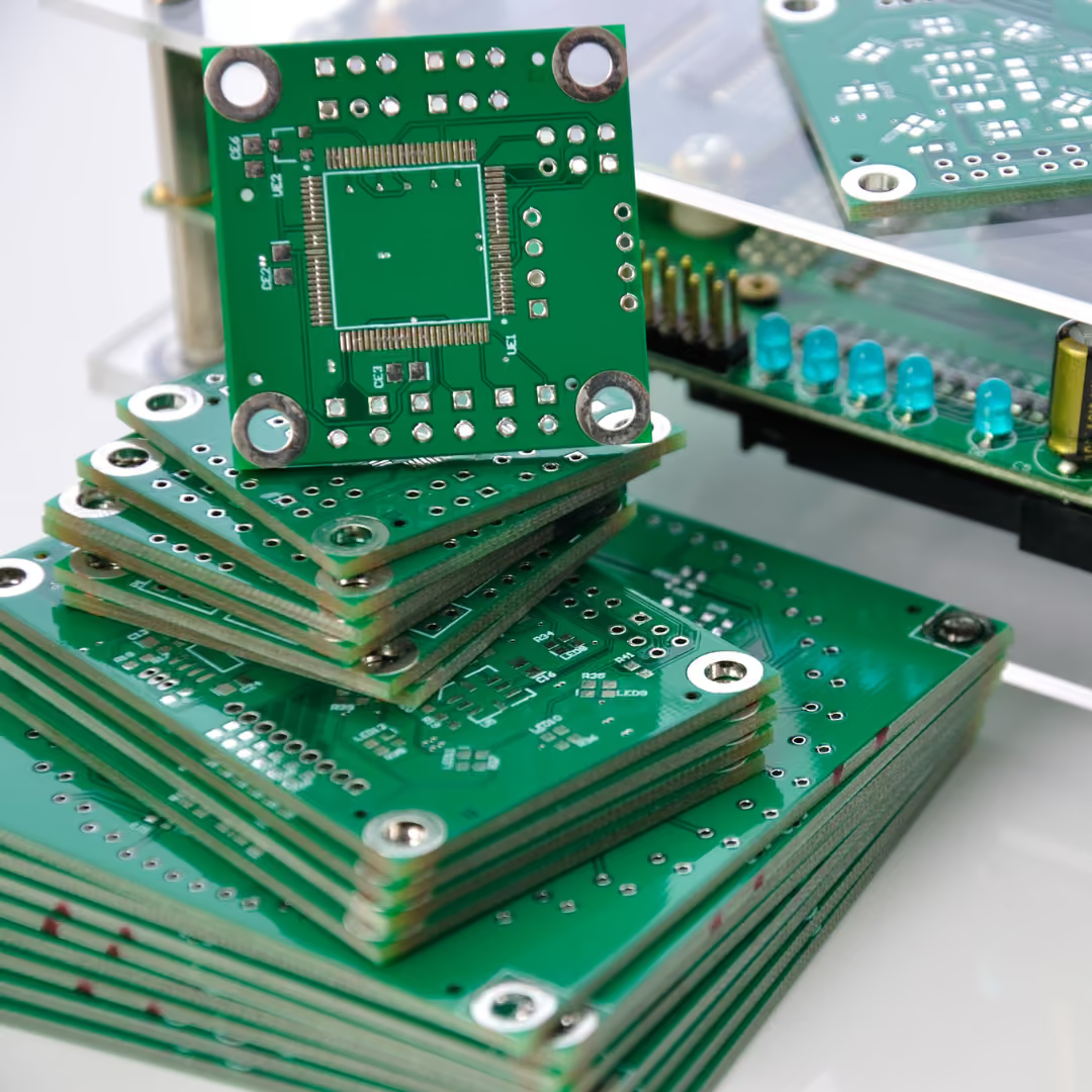
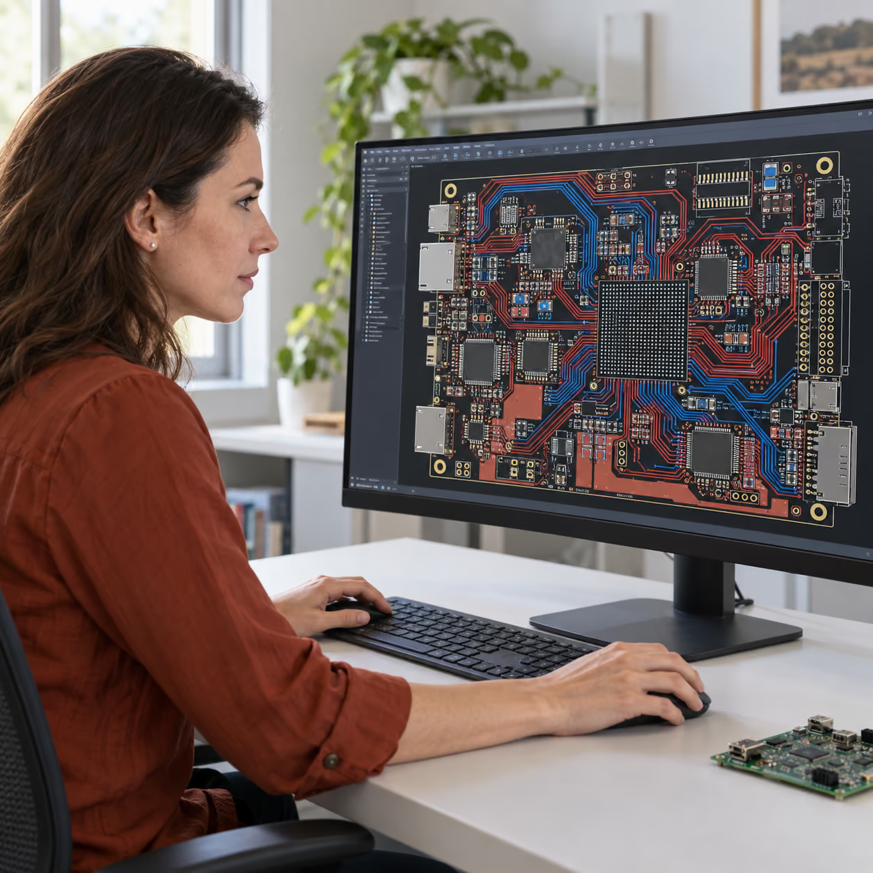
Have production-ready files? Submit your board for a fast quote and production. Need help with materials, stack-up, manufacturability, or a specialized design? Talk directly with our PCB engineering team.


NFR manufactures 1-, 2-, 4-, and up to 8-layer PCBs for prototypes and low-to-medium-volume production, including boards for RF, high-speed digital, mixed-signal, and other demanding applications.
Standard fast-turn capabilities include approximately 2 business days for 2-layer boards and 3 business days for 4-layer boards. Single-layer bare boards can be manufactured the same day, and expedited turnaround may be available for other designs depending on requirements. Lead times for higher layer counts and specialized designs vary based on complexity and material requirements.
Yes. NFR's PCB manufacturing is U.S.-based, providing domestic production, responsive engineering support, and a more secure supply chain.
Yes. Rapid prototypes and low-to-medium-volume programs are a core part of NFR's PCB offering. This makes NFR particularly well suited to engineering development, research, qualification, and specialized production programs.
A list of PCB Materials can be found here.
Yes. NFR supports RF and microwave applications, including high-frequency materials, hybrid stack-ups, controlled impedance designs, and specialized RF structures.
Yes. NFR's broader experience in analog, mixed-signal, RF, and high-speed digital engineering provides additional expertise for boards with demanding signal-integrity and performance requirements.
Available finishes include ENIG, including Bondable Gold Plating, immersion tin, and bare copper. Other application-specific requirements can be discussed with the NFR manufacturing team.
Yes. Bondable Gold Plating is available for applications requiring wire bonding and integration with advanced semiconductor packaging.
Yes. Customers can work directly with experienced engineers to discuss manufacturability, materials, stack-up, and other technical considerations before production.
Yes. NFR manufactures PCBs and specialized substrates, including fine-pitch substrates supporting semiconductor packaging and integration applications.
Yes. Unlike a standalone PCB fabricator, NFR can also support ASIC development, wafer dicing, packaging, cleanroom processing, testing, bring-up, and production support.
Yes. NFR supports fine-feature substrates and specialized interconnect development for projects with demanding integration requirements. The work may include design, simulation, test structures, samples, and prototype builds to evaluate the proposed approach.