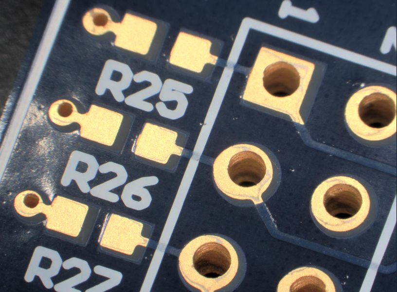
A PCB can pass DRC, match the schematic, and still fail at the fab. Before release, verify the design against the fabricator's stock materials, tolerances, and process capabilities. The goal: a board they can build from the package alone, without calling you.
Board outline: Confirm dimensions, cutouts, slots, and radii are consistent across PCB data, fab drawing, and manufacturing files. Conflicts stop CAM review.
Stackup & materials: Validate required core thicknesses, prepregs, copper weights, dielectrics, and finished thickness with the fabricator. If a specific material is required, call it out explicitly. If equivalents are acceptable, define which properties must hold.
Copper weight & distribution: Confirm copper by layer and review distribution across the stackup. Heavy or uneven copper affects etching, plating tolerances, and bow/twist.
Trace width & spacing: Flag geometry near the fabricator's process limits. Manufacturable isn't the same as within the preferred process window.
Copper-to-edge clearance: Check copper near routed edges, slots, cutouts, and scoring, including internal planes. Registration tolerance eats into effective clearance.
Plane integrity: Review for isolated copper, unintended splits, and small features that create etching problems.
Drill sizes & annular rings: Review finished-hole sizes against drill diameter, plating thickness, and registration tolerance together. Tight annular rings turn normal variation into breakout.
Aspect ratios: Compare hole diameter to board thickness against the fabricator's plating capability. High aspect ratios risk non-uniform plating and long-term reliability issues.
Blind, buried & filled vias: Confirm structure, sequential lamination requirements, fill type, plugging, capping, and planarization before the stackup is locked.
Specify target impedance, tolerance, and relevant layers. Let the fabricator tune trace geometry to the actual production stackup; locking geometry while specifying impedance removes their ability to compensate for real copper and dielectric properties. For differential pairs, review width, spacing, reference plane, copper thickness, and dielectric together.
Solder mask: Check clearances, dams, via treatment, and fine-pitch footprints. Features below registration limits cause missing dams and mask encroachment on pads.
Silkscreen: Verify reference designators, polarity marks, and pin-one indicators clear pad edges. Clipped markings become assembly and inspection problems.
Surface finish: Select based on component technology, assembly process, shelf life, and reliability requirements. ENIG, HASL, OSP, ENEPIG, and immersion silver each carry different implications for fine-pitch assembly, wire bonding, flatness, and cost.
Panelization: Consider board geometry, edge components, routing method, scoring, fiducials, and tooling holes. Let the fabricator optimize the production panel where possible.
Test: Confirm test-point accessibility and define electrical-test requirements beyond the fabricator's standard process.
Review Gerber/ODB++ data, drill files, netlist, stackup, fab drawings, and notes as a set. Conflicting requirements between the drawing, stackup, and manufacturing data force CAM to stop and ask. Run automated DFM checks, but they catch rule violations, not whether all manufacturing decisions make sense together.
The real test: Could CAM and process engineering build it correctly from the released package, without calling you? If the answer is "they'll know what we mean," it isn't ready.
NFR combines U.S.-based PCB manufacturing with engineering support from people who understand both design and fabrication. Order here.