mOSAT Solutions Overview
We support advanced assembly, packaging, and post-fabrication integration paths that help move silicon into robust, manufacturable system-level solutions.
NFR is redefinging Outsourced Semiconductor Assembly and Test (OSAT)
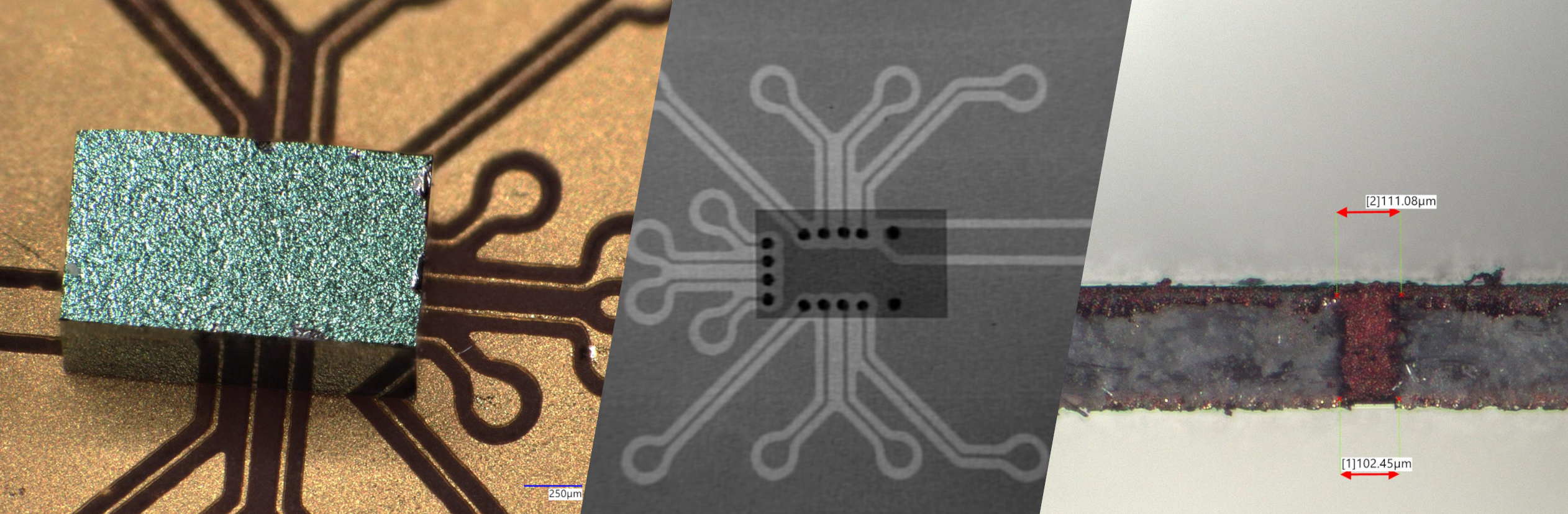
Our U.S.-based mini OSAT provides advanced packaging and test services designed to meet today’s most demanding semiconductor needs. We specialize in fine-pitch substrates, multi-layer PCB/packaging trials, and advanced interconnect technologies including flip chip, wire bond, and 2.5D integration. With local engineering support and rapid prototyping capabilities, we enable faster design cycles, reduced logistics complexity, and greater supply chain security. By combining flexibility with cutting-edge assembly and test expertise, our mini OSAT empowers customers to bring innovative products to market with speed, precision, and reliability.
NFR has expanded its expertise into the OSAT space with the launch of our U.S.-based mini OSAT (mOSAT) operations. Over the years, we have supported companies of all sizes with advanced packaging and substrate solutions, ranging from standard wire-bond packages to complex multi-layer, fine-pitch designs with flip-chip and stacked integration. Having witnessed the evolving demands of the semiconductor supply chain, we are well-positioned to guide you toward the right packaging and test technologies to ensure reliable delivery for your target applications and markets
Our Products
Advanced Packaging
Flip-chip, 2.5D interposers, fine-pitch assembly, and high-density routing for performance and size.
Explore Advanced Packaging →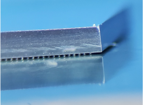
Substrates & Interposers
Multi-layer organic substrates, fine lines/spacing, and build-up for high I/O density.
Explore substrates →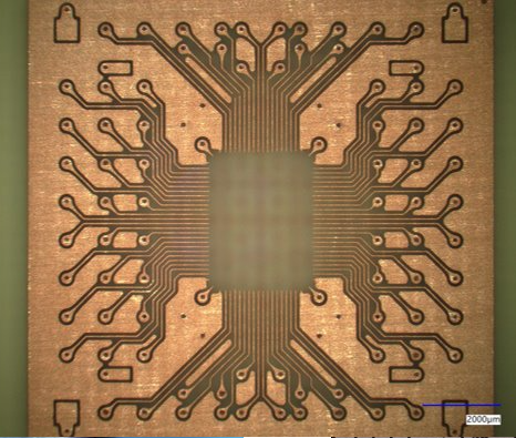
Wire Bond Packages
Cost-effective QFN/QFP and custom leadframe solutions with reliable Au/Al/Cu bonding.
Explore Wirebonding →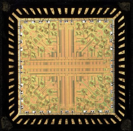
RF Structures
RF structures Fab service provides a micron level accuray of rapid prototyping dual layer interposer.
Explore RF Extructure →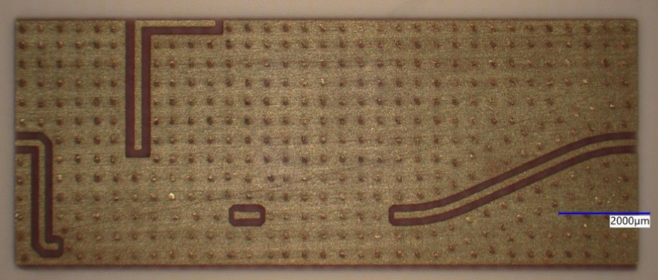
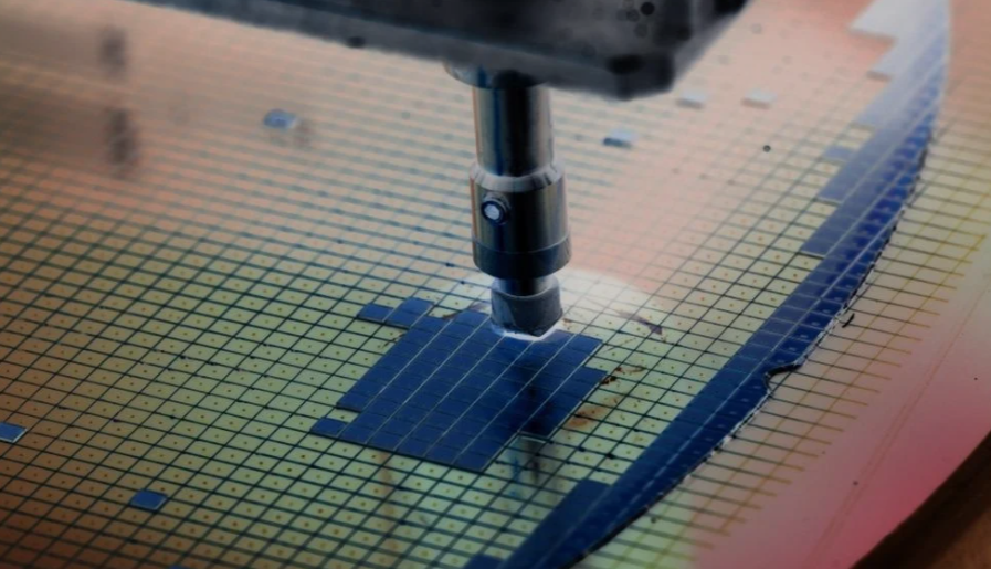
Dicing Services
High-precision wafer dicing services with narrow kerf cuts supporting silicon, glass, and advanced substrates.
Explore Dicing Services →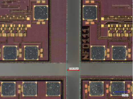
Full Service
Package test, burn-in, characterization, and custom handlers/fixtures for fast verification.
Explore Full Service →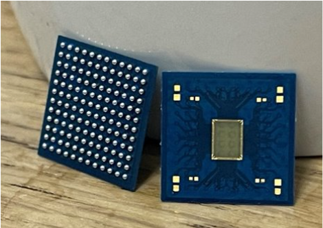
mOSAT by NFR
Agile. Local. Advanced. Redefining semiconductor packaging and test, closer to where innovation happens.
1 Capital cost avoidance
Building and maintaining in-house assembly and test facilities is extremely expensive. mOSATs already have the infrastructure, saving your company from heavy capital expenditures or overseas expensive engagements to reach your semiconductor packaging and prototyping needs

2 Scalability & flexibility
NFR mOSAT concept allows your company to ramp up or scale down production quickly without needing to re-size your facility. We can support a decent volume to get you close or at production level.

3Specialized Expertise
NFR's mOSAT has invested in advanced packaging, test capabilities, and new technologies (e.g., flip chip, fan-out wafer level packaging, 2.5D/3D integration) so that you don't have to. Our customers can leverage this know-how instead of developing it internally.
4Speed to Market
NFR's mOSAT established processes can accelerate your time-to-market by handling assemly and testing in prallel with design and fabrication. NFR offers our customer a unique combination of System, ASIC and Substrate design not before seen in any industry.

5Geographic Reach & Supply Chain Benefits
NFR's mOSAT unlike large offshore providers, has a focused approach allowing us to deliver highly customized solutions, rapid prototyping, and agile support at financially efficient levels locally.